ZoomZoomLuke wrote:Squonk wrote:Thank you!
Following my experience with USB 2.0 EHCI only in the AR9331, a hub is mandatory if you want to use any low or full speed device, and adding a microSD in the same chip would allow a smaller flash capacity and expandable memory for cheap...
Specifically, I was thinking of the AU6350-MGL chip.
But the problem is to get the AR9331 chip, anyway 
Thank you for your brilliant reverse engineering work.
Thank you!
I still need to update the schematic and layout to match latests pictures that also include the internal layers.
ZoomZoomLuke wrote:Do you think we could (legally) adapt these layouts and produce a much more hacker friendly device? Im sure we could squeeze in an extra pinheader or two and reshape the board slightly to fit into a readily available enclosure.
IANAL, but it looks like chip die layouts are protected, but not PCB layouts, as long as you don't include protected contents such as logo or trademarks.
Anyway, this layout is probably largely inspired by the Atheros AP121 reference design.
Yes, first, we should provide an easier access to the console 
Second is to increase SSDRAM/Flash size.
Then, given the problem we found on the USB I/F, an USB hub chip would be of utmost importance to me, in order to connect low/full speed devices like POTS modems, GPS, Arduino boards, USB-UART converters and all kinds of home-built devices.
And of course, fan out all the available pins (I2S, SLIC, additional Ethernet ports, JTAG, etc.) to headers!
ZoomZoomLuke wrote:Obtaining the AR9331 is not a problem, my company has these in stock from producing military ethernet modules so I could purchase them for about $8 each for single pieces. Would this make such a project feesable?
Yes, but the challenge would be to produce the boards!
The PCB is 4-layer, so we cannot use the cheap PCB prototype services. So we will need to find one PCB house that can do this cheap, and also provide the solder paste stencils.
For this kind of board, hand assembly with a soldering iron is not possible. Given the AR9331's dual-row pinout, hot air is not trivial, so a reflow oven is recommended. You can find those starting at $100-150, but it means not everybody can put together the board by him/herself.
Maybe taking a layout where all the components are on the top PCB side is a also good idea...
For manufacturing, we need to find an easy way to Flash the bootloader into Flash memory, then write a software that performs the board self-tests.
Then, the RF part is probably very tricky, as the exact values for the RF matching network are to be tuned, depending on the board layout, etc.. Then the RF needs to be calibrated using the ART (Atheros Radio Test) software (which I don't know how to get, except by signing and NDA with Atheros) and corresponding tuning values written into Flash memory during manufacturing.
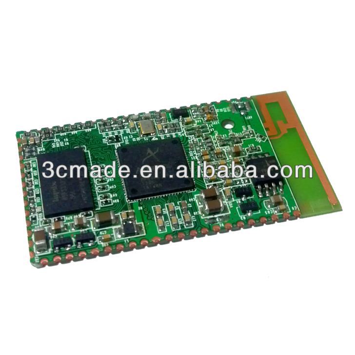
Also, consider that there are AR9331-based SMT modules starting to appear in China for about the same price as a TL-WR703N, with more or less GPIOs... They do not provide all the connectors for Ethernet, antenna, USB, etc, but this may be seen as an alternative to making our own board...
But this could also make a nice Kickstart/Indiegogo (I am not US or UK-based) campaign!


