OpenWrt Forum Archive

Topic: TP-Link TL-WR703N Reverse Engineering

The content of this topic has been archived between 22 Mar 2018 and 21 Apr 2018. There are no obvious gaps in this topic, but there may still be some posts missing at the end.

Despite its interesting characteristics, the TL-WR703N router suffers from a complete lack of information regarding its implementation:

  • The datasheet for the main chip (Atheros AR9331) is only available under NDA (Non-Disclosure Agreement)

  • No available schematic, layout or BOM (Bill Of Materials) files

There are already several OpenWRT forum threads dealing with hardware hacking of the TL-WR703N, and they tend to rapidly focus on the research of available I/O resources and low-level electronic understanding. Although some progress has been made, like an almost exhaustive main AR9331 chip pinout and a component-by-component description, only a full reverse-engineering work can provide the answers to all the questions on the hardware.

This is the reason why I undertook the job of reverse engineering the TL-WR703N using EagleCAD, and here is the result so far:

TL-WR703N PCB Top in EagleCAD
TL-WR703N PCB Bottom in EagleCAD

All the details can be found on the:

corresponding Github Page

.

All design files are available at https://github.com/Squonk42/TL-WR703N.

The next step will be to recreate the full schematic from this layout.

Please let me know your comments about all this here!

(Last edited by Squonk on 13 Oct 2012, 09:37)

Very nice work Squonk!

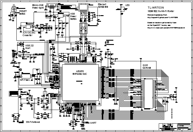
Here it is: the almost complete TL-WR703N schematic, reverse-engineered from the PCB layout obtained from Kean's Hi-res PCB pictures:
TL-WR703N PCB Top in EagleCAD

All the details can be found on the:

corresponding Github Page

.

All design files are available at https://github.com/Squonk42/TL-WR703N.

Right now, the internal layers have not been taken into account, thus the round markers on the schematics and PCB corresponding to vias going to unknown internal layer traces. If you want to help, please let me know where they are going!

Please let me know your comments about all this here!

First, the schematic is not complete, since it is only based on the observation of the external layers. The circle markers with 0-9/A-Q labels in the schematic are vias going to internal layers, and they match the yellow dots with the corresponding labels on the PCB layouts. If you have some time and the required electronic knowledge, this is something you can try to investigate wink

In order to locate things inside the schematic, I propose you to use the schematic external frame row/column position: for example, the main AR9331 U1 chip is located in E4-F5 and SPI FLash chip U3 is in E2.

Yes, there are a lot of unused pins on the AR9331, but they are not all available GPIOs. Some of them have dedicated functions, like the second RF interface connected to GND in area G4, or the unused additional Ethernet ports located in D4.

There are some unused GPIOs used for other TP-Link models (TL-MR3020) located in D5, but they are not accessible since they are located beneath the AR9331 chip.

So the only available pins usable for GPIOs are the ones we already know: those located in E3: GPIO11 (RESET_SW), GPIO7, GPIO6 (LDO, which is actually !USB_OC for USB overcurrent indicator), GPIO29, GPIO8 (USB_POWER) and GPIO27 (LED3); those located in G4-5: GPIO28, GPIO13 to GPIO17, GPIO0, GPIO1 and of course the TP_IN/TP_OUT LVTTL UART pins.

But most of them are tied either to GND or VCC by a pull-up/pull-down resistor, and most of them are used as boot-time configuration switches, so you must be careful as they cannot be set to the other state, at least during boot. This is why I tried to unsolder them one by one and tie them to the opposite level, and see if it prevents the router from booting tongue

This is a second area of investigation, from my previous post, I guess that by changing these boot-time switches, it is possible:

  • to boot using the MDIO bus. Maybe also boot from USB? Bootstraping from ROM directly to USB (DFU ?) could be nice to recover devices with bricked U-Boot big_smile

  • that the normal 25 MHz crystal can be overclocked to 40 MHz

  • to select USB to work in host or device mode

  • to boot from SPI and probably also internal bootstrap ROM, if booting from SPI is optional

  • to disable SDRAM and choose between DDR1 or DDR2, or maybe select the correct SDRAM/DDR1/DDR2 config

Anyway, there are some very interesting points that can be seen from this schematic:

  • by removing J1, you can solder an external antenna

  • by populating R113, you can bypass the USB current-limited power distribution siwtch U6 and thus supply the TL-WR703N from the USB A connector

  • by removing R65/R68, you have access to the Ethernet 1/2 and 4/5 pairs to use as PoE to supply the device

  • by disabling first the USB in the kernel, you can use the USB_POWER signal to control the USB Host connector supply and thus control an external static relay without any soldering smile

(Last edited by Squonk on 13 Oct 2012, 09:38)

yea im see it's not finish,but it's a lot fun,im broken 1wr703,2mr11u,with this,i can get a lot help,so im can fix it:) it's really great!

what's mean ddr2,what's it use for?

What would be nice is to X-ray a bare TL-WR703N board to see the internal layers smile

X-ray machines are commonly used for controlling BGA chips, so you can find them at electronic assembly factories with BGA capabilities, or in some electronic labs.

DDR2 is the SDRAM type: in embedded systems, you can find SDR (Single Data Rate) SDRAM clocking data on either the rising or falling edge of the clock signal, DDR (Double Data Rate) or DDR1 SDRAM clocking data on both clock edges, and DDR2 provides higher bus speed and half internal clock speed, thus doubling the transfer rate, see http://en.wikipedia.org/wiki/DDR2_SDRAM.

The TL-WR703N uses DDR1 SDRAM.

(Last edited by Squonk on 13 Oct 2012, 13:49)

Amazing work! I'm currently struggling with my 2nd 64mb upgrade (freezes often,reboots etc...) and it may be I have a dead unit that could be depopulated and used for "the cause".

Thanks!

But having a bare PCB is only useful if you can get access to an electronic X-ray facility...

The other solution is to grind down the PCB to access the internal layers one by one like this:
http://bb.osmocom.org/trac/wiki/PirelliDPL10/PCB

oh imsee ddr2 just the speed:) i thought is like the with 2x ddr,so make it to 128M haha

the ar9931 is a lot blink pin,cant let them out,them just keep in the hole,never have chance to come out

the crystal ,if make it to 50mhz,what's happen?

As we don't have the AR9331 datasheet, it is impossible to tell!

It will probably not work, since the crystal is used by an internal PLL, and changing the crystal frequency would require to modify the firmware (bootloader and kernel) to adjust the PLL settings.

Because of the PLL which already multiply the crystal frequency, increasing the crystal frequency does not necessarily implies that you will increase the system frequency.

(Last edited by Squonk on 14 Oct 2012, 10:14)

Cool job!

The RF part have some differential circuit,but it's not clear from your SCH plot.

What do you mean?

You can see clearly the differential RF signals connected to U1's A62 to A65 pins, with separate differential paths for TX and RX, joining into a common differential path before getting unbalanced into J1, then to the antenna's foot capacitive impedance divider...

You can even tell about the impedance-terminated second RF antenna path connected to A68/A69 and probably A70/A71 too.

Do you have suggestions on how to improve the schematic?

(Last edited by Squonk on 14 Oct 2012, 14:08)

I know little about the HW,no PCB layout experience.So i only can understand some very very clearly SCH.
The differential RF signals should be changed to single ended signals,but from the SCH,i can not see where the "join" point.

The Electronic Component on differential RF signals should be symmetrical,so the two "J" and the "c18","c24","c85" also not verify clear for me.

I suggest not plot the SCH in one page,divide to different page with different function,just like the POWER part,the RF part,the DDR part,the USB part,the ETHERNET part,the GPIO part.Though the WR703N is verify simple to plot in one page,it's more clear to plot it in different page.

OK, I understand what you mean now!

The 2 "J" are vias going to the internal layers, and they are at the same potential ans the "K" and "O", I suspect +3.3 V, so C18/C24 andC85 are just decoupling capacitors, and you can consider that C18 is // to L4 and C24 // to L2 if you want, and that the higher value C85 is just a chip decoupling capacitor close to the AR9331 chip.

I also rechecked the schematic and PCB, and thanks to slboat from the forum, I spotted the missing connection you are speaking about: there is a wire between C27/C28 and L3/C21: it is your "join" point!

Sorry, but the single page schematic is not a choice, as the free version of EagleCAD used does not allow you to have more than one schematic page sad

That's why I tried to label the different schematic parts and separate them as much as possible. You just have to zoom in/out as required smile

I updated the files to Rev. B to correct the problems found so far:

  • missing wire in RF section between C21 and C28 + cleaned up RF section (thanks mips & slboat!)

  • missing wire between U1-A33 and +2V5

  • probed all vias going to internal layers with a DMM, as labs or fabs with X-ray machines are closed on sunday smile

It turns out that most of the vias can be guessed easily, so there is only one remaining ("L") which looks like it's tied to +3V3, but that I don't understand.

If someone gets a clue, please let me know!

About the "L",try to check if this is help:
http://www.zlgmcu.com/mxic/NOR_Flash_c/img/MX25L1605D_yy.jpg

Yes, the S25FL032 (U3) connections are otherwise pretty much the same as the schematic you provide:

  1. !CS is driven directly by an AR9331 pin

  2. SO/IO1 is S25FL032 data serial output, and goes through a 3/4 voltage divider made up of R57/R60 to adapt the 3.3 V output to the AR9331's 2.5 V input level

  3. !W/ACC/IO2 is the write protect and is pulled up by R62 to 3.3 V, as R63 is not populated, so it is the same as your R2

  4. the GND pin is connected to GND smile

  5. SI/IO0 is S25FL032 data serial input, and comes straight from the AR9331, as the low/high voltage thresholds are compatible

  6. SCK is the S25FL032 input data clock, coming from the AR9331 too

  7. !HOLD/IO3 is where the question is: both schematics feature a pull-up resistor, but in my case, this resistor is split in 2: R58/10k and R95/10 ohms, with the famous "L" label in-between. Yours is just a standard 4.7k (R1) pull-up resistor

  8. VCC is the power supply, properly decoupled by a 100nF capacitor (C7 or C1 in your schematic)

I don't see the point in having 2 series pull-up resistors for the !HOLD/IO3 signal in the TL-WR703N. What is strange is to use a rather "large size" 0603 resistor with such a small value?!?

Maybe it is something related to manufacturing, such as way to program the SPI Flash in situ, then mounting the 0603 R95 resistor afterwards? I read the "QUAD Page Program (QPP)" section 9.15 in the S25FL032 datasheet, but in this case, the !HOLD/IO3 is used as IO3 parallel input, and the series R58/10k is not appropriate. Moreover, there should be the same configuration for the other IOx pins, too.

The S25FL032 also features an OTP (One Time Programming) Flash region, but the !HOLD/IO3 has nothing to do with it.

So I still don't know the purpose of this "L" via to internal layers.

(Last edited by Squonk on 20 Oct 2012, 09:10)

Squonk wrote:

You can even tell about the impedance-terminated second RF antenna path connected to A68/A69 and probably A70/A71 too.

Would it be possible to wire to a socket for an optional external antenna here, while keeping the internal antenna operational?

sturle wrote:
Squonk wrote:

You can even tell about the impedance-terminated second RF antenna path connected to A68/A69 and probably A70/A71 too.

Would it be possible to wire to a socket for an optional external antenna here, while keeping the internal antenna operational?

Doubtful. If you look at the components required on the existing antenna, there are quite a lot of them. And some are ultra-low valued capacitors and selfs, sot it would be very difficult to just reproduce as is on a different PCB.

Your best guess would be to try the TL-MR3020, which has almost all these components already mounted, just missing a jumper.

However, the stock MR3020 only uses a single antenna, and it may be because of power dissipation problems in the AR9331 chip itself, so be careful!

Notwithstanding the software side, which would required WLAN driver modifications to enable antenna diversity.

Squonk wrote:

Yes, the S25FL032 (U3) connections are otherwise pretty much the same as the schematic you provide:

  1. !CS is driven directly by an AR9331 pin

  2. SO/IO1 is S25FL032 data serial output, and goes through a 3/4 voltage divider made up of R57/R60 to adapt the 3.3 V output to the AR9331's 2.5 V input level

  3. !W/ACC/IO2 is the write protect and is pulled up by R62 to 3.3 V, as R63 is not populated, so it is the same as your R2

  4. the GND pin is connected to GND smile

  5. SI/IO0 is S25FL032 data serial input, and comes straight from the AR9331, as the low/high voltage thresholds are compatible

  6. SCK is the S25FL032 input data clock, coming from the AR9331 too

  7. !HOLD/IO3 is where the question is: both schematics feature a pull-up resistor, but in my case, this resistor is split in 2: R58/10k and R95/10 ohms, with the famous "L" label in-between. Yours is just a standard 4.7k (R1) pull-up resistor

  8. VCC is the power supply, properly decoupled by a 100nF capacitor (C7 or C1 in your schematic)

I don't see the point in having 2 series pull-up resistors for the !HOLD/IO3 signal in the TL-WR703N. What is strange is to use a rather "large size" 0603 resistor with such a small value?!?

Maybe it is something related to manufacturing, such as way to program the SPI Flash in situ, then mounting the 0603 R95 resistor afterwards? I read the "QUAD Page Program (QPP)" section 9.15 in the S25FL032 datasheet, but in this case, the !HOLD/IO3 is used as IO3 parallel input, and the series R58/10k is not appropriate. Moreover, there should be the same configuration for the other IOx pins, too.

The S25FL032 also features an OTP (One Time Programming) Flash region, but the !HOLD/IO3 has nothing to do with it.

So I still don't know the purpose of this "L" via to internal layers.

As I know,the flash are already programed some manufacturing code before SMT.
So it's really strange about the "L".
A small resistor(R95) connect to v3.3,its' seems it want to filter something to get a more clear v3.3?or add it for pass some hardware test?But why it then connect to R58?
If the "L" is connect to C7,and R95 is not connect to R58,but used some else where?

I could try to grind down the PCB of a TL-WR703N and scan the single copper layers? Like Squonk already explained. I have access to some machines and enough craftsmanship. I think it's worth a try and I am happy to donate one TL-WR703N.

Please let me know if this is still needed for finishing or verifying the schematics.